Our ALD (Atomic Layer Deposition) equipment plays a crucial role in semiconductors, optics, MEMS, and photovoltaics, delivering ultra-uniform, high-conformality thin films with atomic-level thickness control.
It ensures precise and defect-free coatings even on complex 3D structures, deep trenches, and high-aspect-ratio components, making it an ideal solution for next-generation technology.
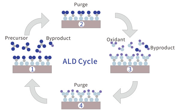
ALD is a type of CVD technology. It alternately introduces different chemical vapor precursors, conducts self-limiting chemical reactions on the substrate surface, and finally deposits thin films layer by layer, ensuring precise thickness control.
Precise Thickness Control You can think of the process as "adding a blanket one layer at a time," where each cycle deposits a single atomic layer, allowing precise control over film thickness during deposition.
Highly Uniform & Conformality This step-by-step growth enables ALD to form highly uniform films on complex or high aspect ratios structures, preventing excessive accumulation and ensuring complete coverage in every corner.
TALD & PEALD Available
TALD uses thermal sources to heat precursor gases for atomic layer deposition, is suitable for high-temperature deposition. PEALD, on the other hand, uses plasma to excite precursor gases, allowing deposition at lower temperatures, more suitable for temperature-sensitive materials.
We offer tailored atomic layer deposition solutions and equipment configurations based on your specific needs
Turnkey Solutions
We provide high-quality, stable, and reliable equipment, offering full support throughout the entire lifecycle, covering all aspects from design and installation to maintenance
Rich Expertise With 19 years of expertise in vacuum coating, we have honed deep technical knowledge to address the most challenging coating requirements with precision and efficiency
Custom ALD Solution For Your Business
If you are in the semiconductor, optics, MEMS, or photovoltaics field and need to deposit films on complex structures, ALD is your ideal solution. Our equipment offers precise control over film thickness, excellent uniformity, and conformal coating on high aspect ratio structures. Contact us today to explore how our ALD technology can meet your needs!