Widely applied in electronic device R&D and production, it allows metal or resistive film deposition on ceramics, glass, and metals. Capable of full-coverage plating for through-vias, with TGV aspect ratios up to 15:1 and TCV vias of 20 µm diameter at aspect ratios up to 20:1.
Adopts a load-lock sputtering system with modular options for RF, DC, HiPIMS high-power pulsed magnetron sputtering, and pulsed bias. The transfer chamber supports up to five substrate carriers with automatic lifting and handling, improving throughput. Multiple cathodes can operate simultaneously for multilayer deposition. The system enables automated process control and comprehensive data logging.
Your Benefit, Our Expertise
Key Features of TGV / TCV Sputtering System
Customization
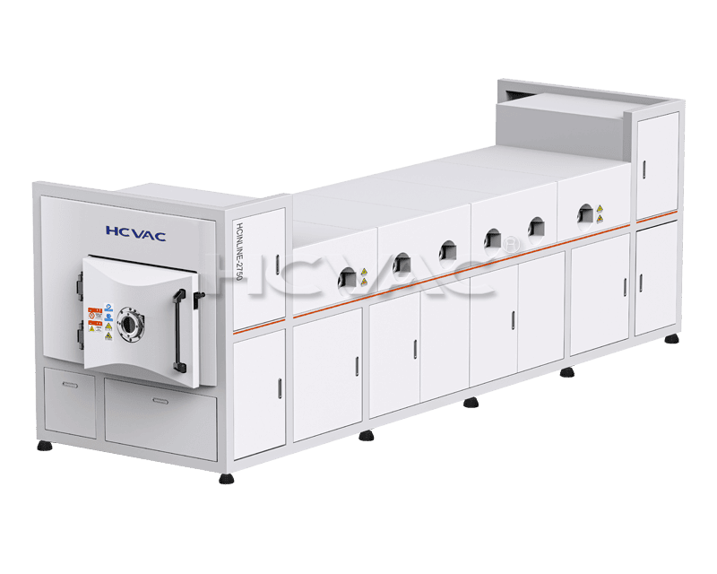
Tailored TGV solutions for your advanced packaging needs
TGV/TSV Process
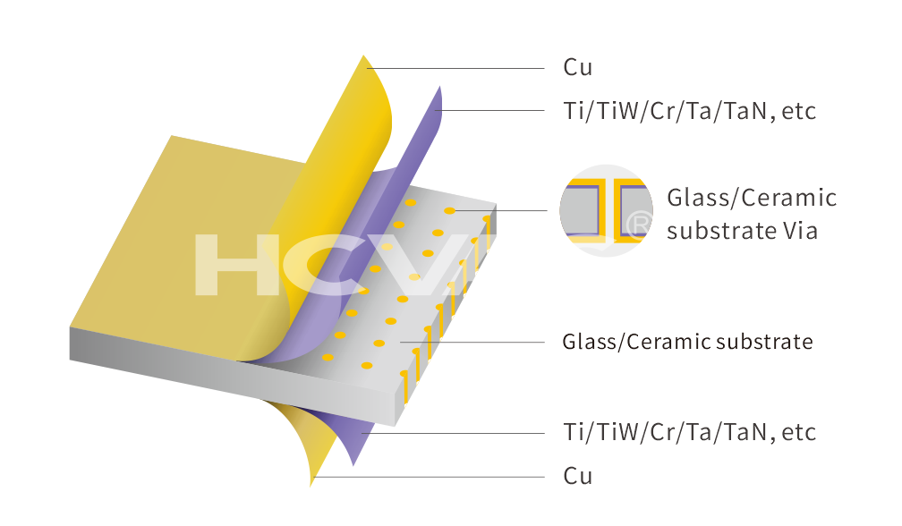
Designed for conductive vias, insulating layers, and seed layers in advanced packaging
Efficient
High productivity at low cost
Future-Ready
Supports smaller sizes and more multi-layer designs to accelerate technology upgrades